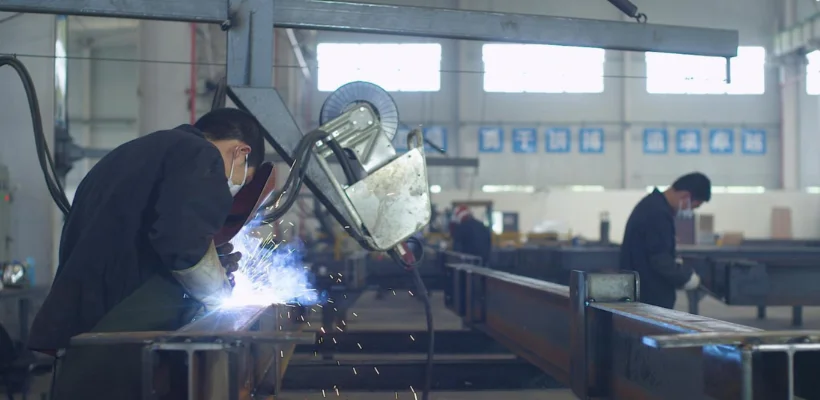
The semiconductor industry is evolving rapidly, driven by miniaturization, performance demands, and material advancements. As manufacturers seek higher precision, efficiency, and sustainability, diamond wire cutting technology is emerging as the future of wafer and substrate processing.
Unlike traditional mechanical sawing, laser cutting, or EDM methods, diamond wire cutting offers superior precision, minimal material loss, and optimized surface finishes—all essential factors for next-generation semiconductor devices.
In this article, we explore why diamond wire cutting is revolutionizing semiconductor manufacturing and how VIMFUN’s cutting solutions are driving this transformation.
1. Precision at the Nanoscale: Meeting Semiconductor Demands
Why Precision Matters in Semiconductor Cutting
As semiconductor devices shrink to nanometer-scale architectures (e.g., 3nm & 5nm chips), the need for precision cutting has never been greater. Traditional wafer slicing techniques struggle with:
❌ Excessive material loss due to wide kerfs.
❌ Heat-induced stress causing microcracks.
❌ Surface roughness requiring extensive post-processing.
✅ Diamond Wire Cutting Advantages:
✔ Micron-level accuracy, meeting the demands of advanced chip fabrication.
✔ Low-stress cutting, reducing microcracks & defects in fragile wafers.
✔ Smoother surfaces, minimizing the need for grinding & polishing.
🔍 What this means: Higher device performance, lower defect rates, and increased wafer yields—essential for AI chips, high-frequency RF devices, and power electronics.
2. Maximizing Yield & Minimizing Waste: The Cost-Saving Advantage
In semiconductor manufacturing, every micron of material counts. Conventional cutting methods lead to significant material loss, reducing yield and increasing costs.
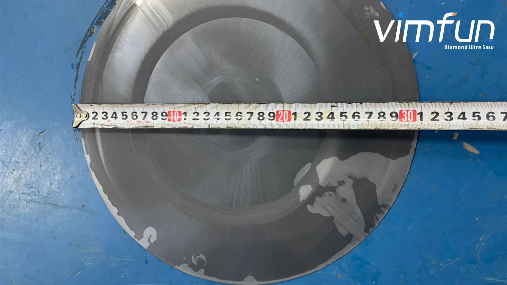
Comparing Material Waste: Diamond Wire vs. Traditional Cutting
| Cutting Method | Kerf Width (Material Loss) | Material Utilization |
|---|---|---|
| Mechanical Sawing | 150 – 200 μm | ❌ 70 – 80% |
| Laser Cutting | 100 – 150 μm | ❌ 75 – 85% |
| Diamond Wire Cutting | 30 – 50 μm | ✅ 90 – 95% |
✅ How Diamond Wire Cutting Maximizes Yield:
✔ Ultra-thin kerf preserves more wafer material, increasing usable substrate count.
✔ Optimized cutting paths reduce waste, lowering raw material costs.
✔ Improved wafer breakage resistance, preventing costly rejections.
🔍 What this means: Semiconductor manufacturers can produce more wafers per ingot, improving profitability and sustainability.
3. The Sustainability Edge: Energy Efficiency & Eco-Friendly Processing
With the semiconductor industry under pressure to reduce its environmental impact, manufacturers must adopt greener cutting methods.
🔹 Challenges with Traditional Cutting:
❌ High energy consumption in mechanical sawing & laser processing.
❌ Excessive slurry waste in abrasive cutting.
❌ Chemical etching requirements increasing hazardous byproducts.
✅ Why Diamond Wire Cutting is a Sustainable Solution:
✔ Reduces energy consumption—diamond wire moves with lower friction, requiring less power.
✔ Eliminates hazardous cutting fluids, reducing chemical waste disposal.
✔ Less slurry contamination, making it easier to recycle semiconductor-grade materials.
🔍 What this means: Semiconductor fabs adopting diamond wire cutting can lower their carbon footprint while improving efficiency.
4. Cutting Silicon Carbide (SiC) & Emerging Materials: The Power Electronics Revolution
As electric vehicles (EVs), renewable energy, and 5G infrastructure expand, the demand for SiC wafers is skyrocketing. However, SiC is one of the hardest materials to process, making traditional cutting methods inefficient and costly.
Why Diamond Wire Cutting is Ideal for SiC Wafer Processing
✅ Handles extreme hardness (Mohs 9.5)—mechanical sawing wears out too quickly.
✅ Reduces kerf loss—more usable SiC wafers per boule, lowering costs.
✅ Prevents microcracking—ensures SiC wafers maintain high electrical performance.
🔍 What this means: EV power modules, 5G base stations, and high-frequency chips can be manufactured faster and with higher reliability.
Real-World Impact: How VIMFUN Helped a Leading Semiconductor Manufacturer
A global chipmaker faced high defect rates and material waste when processing silicon wafers and SiC substrates. After switching to VIMFUN’s diamond wire cutting machines, they achieved:
📉 40% reduction in material waste—lower kerf width saved more usable wafer material.
⚡ 50% increase in cutting efficiency—higher throughput improved fab productivity.
💰 30% cost savings in processing—less downtime & extended machine lifespan.
📈 Higher device performance—crack-free wafers improved chip reliability.
One of their engineers shared:
“Diamond wire cutting allowed us to scale SiC wafer production without increasing costs. The precision and efficiency gains have had a major impact on our semiconductor yield rates.”
Why VIMFUN’s Diamond Wire Cutting is Leading the Semiconductor Industry
For semiconductor wafer manufacturers, VIMFUN’s diamond wire cutting machines provide:
✔ Nanometer-precision cuts for advanced node devices.
✔ Low-stress, crack-free slicing, reducing material waste.
✔ Industry-leading AI automation for real-time process optimization.
✔ Superior sustainability, eliminating hazardous cutting fluids & energy waste.
✔ Versatile material processing, handling Si, SiC, sapphire, and compound semiconductors.
🔹 If you manufacture semiconductor wafers, power electronics, or photonic devices, VIMFUN’s cutting technology will help you stay ahead in high-precision manufacturing.
Conclusion: The Future of Semiconductor Cutting is Diamond Wire Technology
With the semiconductor industry demanding higher precision, lower costs, and sustainable solutions, diamond wire cutting is becoming the gold standard for wafer slicing and substrate processing.
By adopting VIMFUN’s cutting-edge technology, semiconductor fabs can:
✅ Increase wafer yield while reducing material loss.
✅ Eliminate defects and ensure higher chip performance.
✅ Lower energy consumption and minimize environmental impact.
💡 Want to optimize your semiconductor cutting process? Contact VIMFUN today for a custom consultation and equipment demonstration.